Optimizing Input Filter Design for POL Buck Converters
Learn more about POL Buck Converters and optimal input filter designs for reliable on-board power systems, including ripple challenges and EMI considerations.
Download PDFIn the modern day on-board power the Intermediate Bus Architecture (IBA) is the most widely used approach. The input AC or DC input voltage is converted to and Intermediate Bus Voltage (IBV). By far the most popular for IBV is 12V.
The IBV is distributed through the on-board power system and further converted to the desired low voltage.
The switching regulator employed for this conversion is called Point of Load (POL) converter. The POL is usually implemented by using non-isolated Buck topology. The Buck based POLs do not have input to output isolation. This means that the input and the output grounds are not isolated. The desired rail voltage is achieved by means of Pulse Width Modulation (PWM).
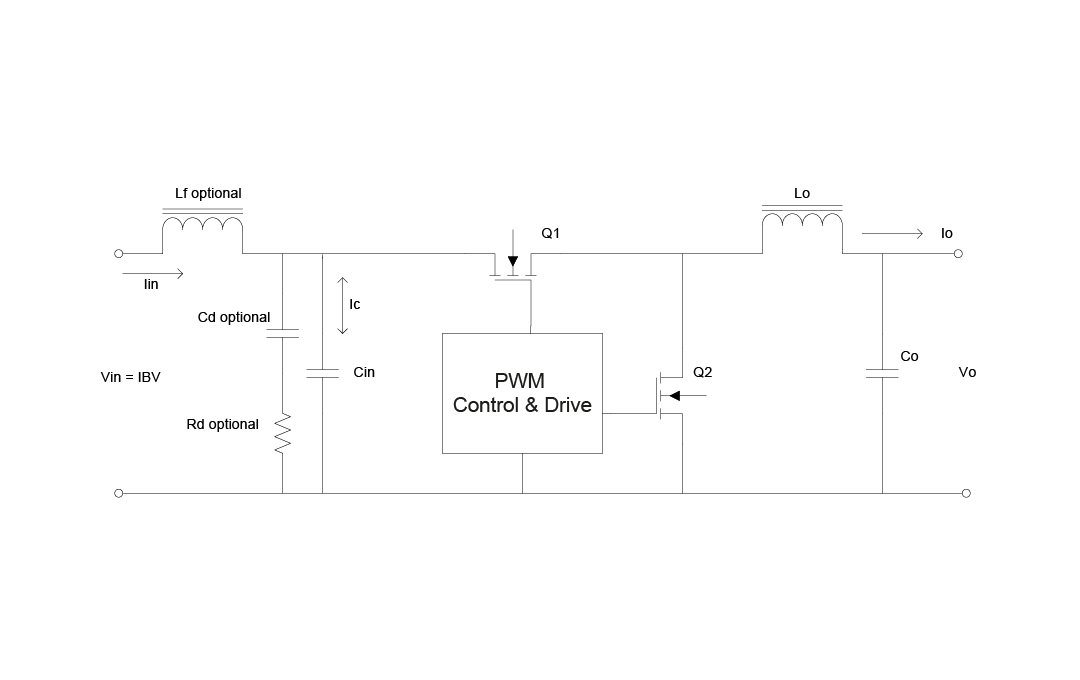
The POL converter has 2 power switches Q1 and Q2 alternatively turn on and off. The upper switch Q1 turns on for time duration determined by PWM control circuit. This voltage pulse is further averaged across the Lo-Co to produce desired output voltage according to equation:
is duty cycle
Image 1: Buck Point-of-load Schematic.
In order to get a better understanding of how this converter operates it is very useful to review and analyze the most important waveforms:
Image 2: Buck waveforms.
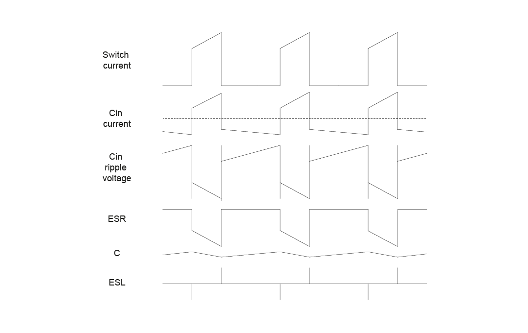
One of the important observations is that the input current drawn by converter is approximately rectangular with a very fast rise and fall times. If not taken proper care the resultant ripple voltage pulses could upset normal operation of local and other converters connected to the same IBV source. In addition the current pulses are also a source of wide spectrum EMI. It is obvious that the input filter is needed to take care of these problems.
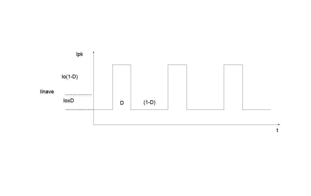
Image 3: Buck input current waveform.
The filtering can be accomplished by adding low-ESR capacitors to the input of the converter.
The input current drawn by converter has AC and DC components. The DC component is the average current drawn from the IBV source and can be approximated by equation:
The AC portion of the input current during the upper switch Q1 on is difference between the output peak current and the input average current:
During the switch Q1 Off the input capacitor is charging with the average input current:
Combining these two expressions we can derive the expression for the RMS current through the input capacitor by taking square root of sum of the and portions charging and discharging of capacitor:
Since capacitors have ESR, AC current passing through them gives rise to self-heating, and hence limits the amount of AC current that can pass through the capacitor with given ESR and size of the package:
As a typical example we can take a converter with the following parameters:
Then the duty cycle:
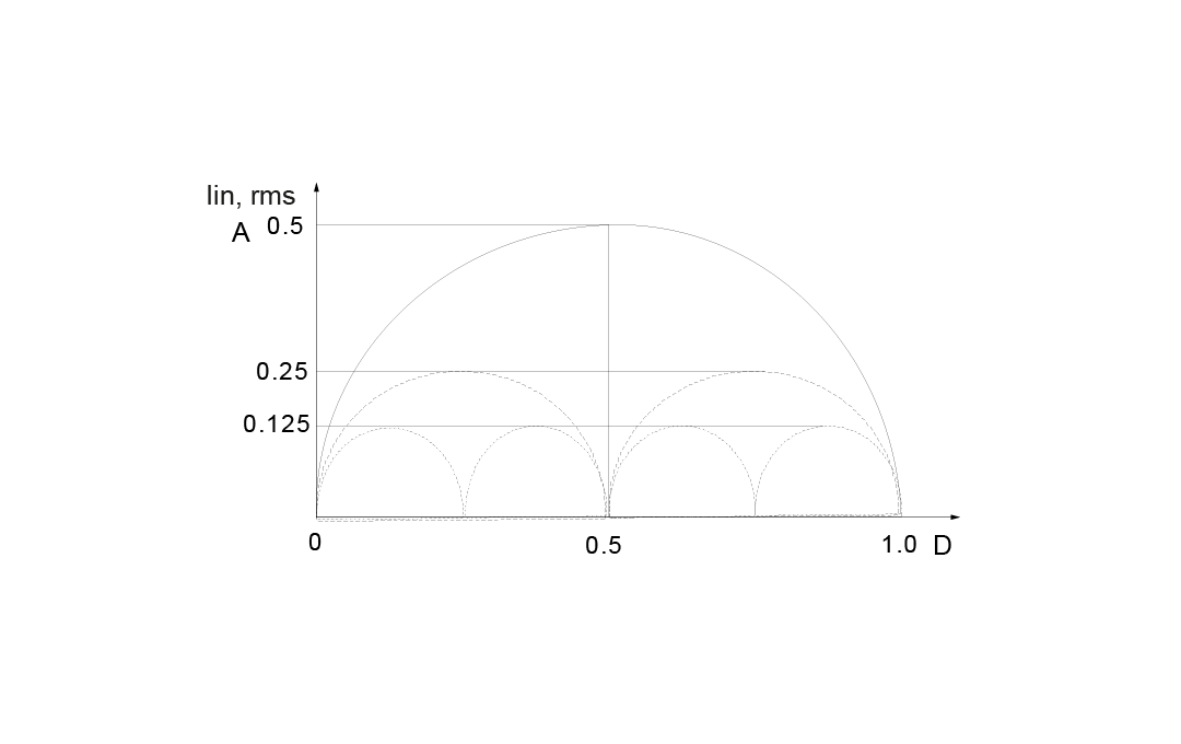
The 330µF, 16V T521 Series High Voltage Polymer Tantalum capacitor has Ripple Current rating 3.1A and ESR = 25mΩ. This means that 2 capacitors in parallel are necessary to handle 6A current. As one can see from the graph the maximum RMS current is at the duty cycle D = 0.5. With low output voltages, the Iinrms is relatively low, but at the same time the input capacitor discharging current Ic- is high. With the conditions in example above:
This ripple voltage has sharp transitions and is very difficult to filter. One of the options is to implement the L-C input filter. Another way is to use multiphase interleaved converters. The input RMS current is going to be reduced as it is shown in Image 4:
Image 4: Input current vs duty ratio.
In order to reduce stress on the electrolytic capacitor and inductive spike, caused the parasitic inductance of electrolytic capacitor, it is always necessary to bypass the electrolytic with the ceramic capacitor. It is also important to estimate voltage ripple across the input capacitors due to the ESR component:
; and the
To calculate the size of the inductor we assume that the IBV end of the voltage is fixed. Then the voltage across inductor can be estimated as:
the value of inductor L is calculated based on desired dl value:
The addition of the input filter to converter will provide control of the input ripple but at the same time can cause the input filter to become unstable and oscillate due to “negative input resistance” of the converter.
Let’s take a look what’s this “negative input resistance” all about. The main function of all “regulators” is to maintain predetermined output parameters (voltage, current, power, etc) regardless of changing input conditions. For example, in case of Linear Regulators, in order to maintain an output voltage they keep the input current constant and the input power raises linearly with the rising input voltage.
This means that the input resistance is positive. In case of switching regulators, the converter draws almost constant input power. This means that the input current is decreased with increasing input voltage and vice versa.
Because ; andThe following graph shows with respect to and :
Image 5: Input current vs input voltage.
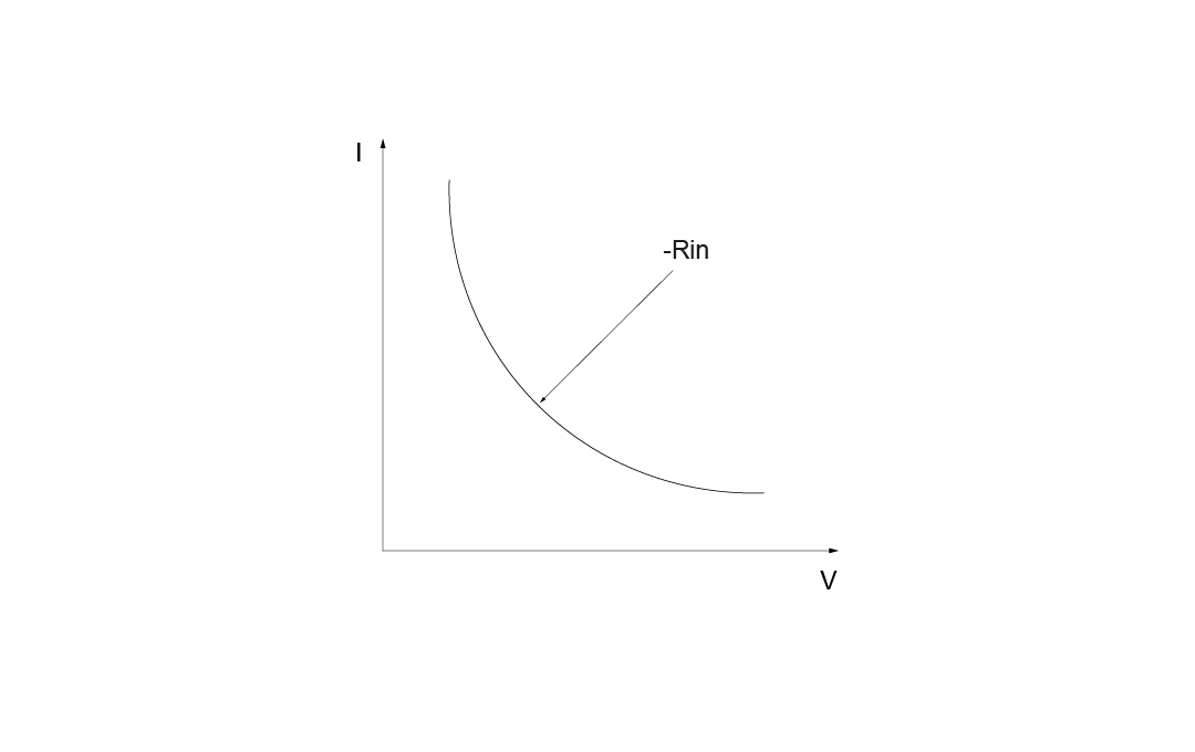
This phenomenon was extensively analyzed by Professor of Caltech, Dr. R. D. Middlebrook. He showed that at certain conditions the converter operation can become unstable because of the input filter and converter interactions. His research led to conclusion that in order to avoid this to happen, the output impedance of the input filter should be lower than the open loop input impedance of the converter, i.e:
This expression is referred as the Middlebrook Criterion. At low frequencies the impedance is calculated at the lowest input voltage and at maximum output load condition:
And critically damped input filter output impedance is:
The following graph shows approximately how the impedances of the converter and the input filter should be separated.
Image 6: Input impedance vs frequency.
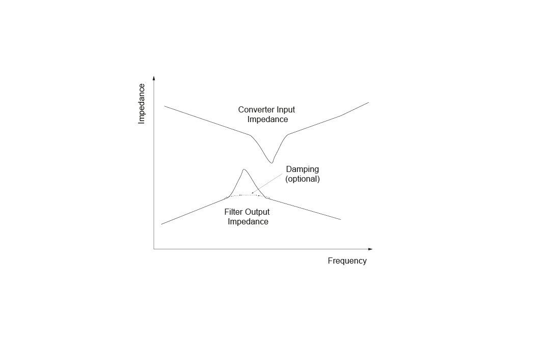
The separation can further enhanced by introducing the damping resistor. One way of doing it is shown in Image 1 and is known as parallel damping.
For critical damping the and are selected:
, and damping capacitor
The real on-board power system is usually comprised of several converters connected to the same IBV source. The interconnection, layout and additional filter components create a very complicated task to solve it analytically. It is therefore very practical to use SPICE to analyze this circuit. Multiple modules should be connected to the common IBV source through the corresponding circuit and parasitic elements.
Image 7: The SPICE Circuit
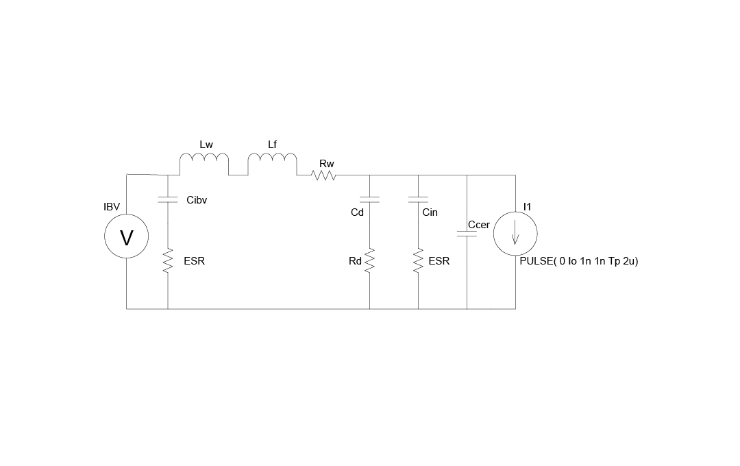
The SPICE circuit in Image 7 represents the single Buck regulator input section.
The current source I1 is a current Pulse with the parameters determined by the actual switching regulator, with the following parameters:
- I1 pulse from 0 to Io
- Pulse rise time tr = 1nsec
- Pulse fall time tf = 1nsec
- Pulse duration
- Switching Period 2µs for switching frequency 500 kHz
View Bel's selection of chokes, coils, and inductors
Learn More